Summary: In this Article, you’ll get to read about —
Assuming you are thinking about what precisely Printed Circuit Boards (PCBs) are and the way in which they are fabricated, then you are in good company. Many individuals have a dubious comprehension of “Circuit Boards”, yet truly aren’t specialists with regards to having the option to make sense of what a Printed Circuit Board is? PCBs are normally used to help and electronically interface the associated electronic parts to the board. A few instances of electronic parts for PCBs are capacitors and resistors. These and other different electronic parts are associated through conductive pathways, tracks or sign follows that are scratched from sheets of copper that are overlaid onto the non-conductive substrate. At the point when the load up has these conductive and nonconductive pathways, the loads up are at times then, at that point, alluded to as Printed Wiring Board (PWB). When the board has the wiring and electronic parts associated, the Printed Circuit Board is presently called a Printed Circuit Assembly (PCA) or Printed Circuit Board Assembly (PCBA).
Printed Circuit Boards are more often than not reasonable, yet are still very dependable. The underlying expense is high because the format exertion demands a ton of investment and assets, however, PCBs are as yet a more expensive full of feeling, and quicker to make for high volume creation. A considerable lot of the business’ PCB Design, quality control, and gathering guidelines are set by the Association Connecting Electronics Industries (IPC) association.
While assembling PCBs, most of the printed circuits are delivered by holding a copper layer over the substrate, here and there on both of the sides, which makes a clear PCB. Then, the undesirable copper is eliminated after the brief cover has been applied by drawing. This main leaves the copper follows that were wanted to stay on the PCB. In the event that the volume of creation is for Sample/Prototype amounts of creation volume, there is a course of different electroplating, which is a complicated interaction that adds follows or a dainty copper layer of the substrate onto the uncovered substrate.
There are different approaches to strategies for subtractive (or the evacuation of undesirable copper on the board) during the creation of the PCBs. The really business technique for creating volume amounts is silk screen printing and visual strategies (Usually utilized when the line widths are fine). Whenever the creation volume is of little amounts, the fundamental strategies for utilized are laser printed oppose, print onto straightforward film, laser opposes removal, and utilizing a CNC factory. The most widely recognized strategies are silkscreen printing, imprinting, and processing. In any case, there is a typical interaction that likewise exists that is usually utilized for multi-facet circuit sheets since it works with the plating-through of the openings, which is designated “Habit-forming” or “Semi-Addictive”.
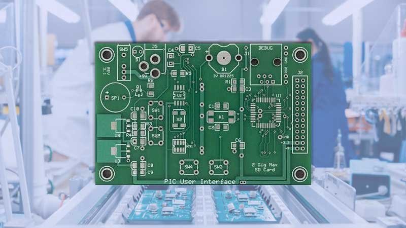
An independent module of interconnected electronic parts shapes a Printed. PCBs or printed are shaped with the assistance of a dainty layer of directing material, either imprinted on a superficial level board, or leading material. Furthermore, a PCB made with populated electronic parts is known as a printed circuit get-together (PCBA or Kingford PCBA).
PCB Manufacturing needs to follow a particular system, remembering every one of the moment subtleties of its plan. To execute the production of the board, you want to follow a few stages. Following are a few stages expected in Circuit Board Manufacturing:
1. Setup
The course of Circuit Board Manufacturing can undoubtedly cause significant damage to you, if not done as expected. Thus, you really want to deal with a few fundamental things like a cycle, material required, client determinations, and most consumer loyalties.
2. Patterning | Etching
The etching doesn’t in a real sense mean etching, yet needs to accomplish something with it. In this, copper and other unprotected regions are uncovered by the engraving oppose film to eliminate the unprotected copper. This leaves the safeguarded copper cushions and follows the setup. Notwithstanding progressed and more current handled use plasma or laser drawing as opposed to involving synthetic compounds for Circuit Board Manufacturing.
3. Engraving Photographs
In this, a photograph veil is joined with compound scratching to take away the copper regions from the printed sheets.
4. Multilayer Pressing
One of the main strides in PCB Manufacturing. This includes adjusting conductive copper and protecting di-electric layers. This helped to frame outboard material.
5. Drilling
Quite obviously, this includes penetrating openings and the data is on put away in the area, where the opening should be bored.
6. Masking
A defensive layer is applied over the copper, which has a meager layer of weld veil and copper follows around it. This is called veiling.
7. Finishing
In this, the cushion regions are covered with a dainty patch layer. This is done to set up the board for wave binding.
8. Electrical Testing
This is the last blow where you are encouraged to actually look at the progression or shorted PCB Manufacturing associations. To do this, you really want to apply a voltage between the focuses.
Read This Also: Where Can You Buy the Top-Quality Petrol Hydraulic Power Packs?